I've decided to open this new thread about PCB (printed circuit board) design using the DipTrace program. This is a continuation of a discussion that developed from an older thread called "Semaphore and 555 Timer Circuit" that seems to have meandered away from its original topic.

I am just getting started with DipTrace and am in need of some guidance from the members of this forum who have more experience with this tool; Gunrunnerjohn, Tom (aka rtr12), and Mjcat have already offered some good advice.

My plan is to make use of DipTrace to integrate an Arduino Nano with various other components for certain model railroad projects that I have in mind. These include ABS signaling, block control, and automated train operations.

To this end, I am just getting my feet wet and will require lots of help.

At this point, I have downloaded and installed the freeware version of DipTrace and am reviewing the tutorial and help system topics. There is also a DipTrace forum available that may be helpful with specific questions. From there I found an Arduino component library that I have also downloaded for use with the program.

Please feel free to offer any advice that you think may help me along in this endeavor.

  -- Leo

Original Post

Replies sorted oldest to newest

So I'm using the schematic editor and want to put some headers in for power connections and other external wiring. And I've found connectors of all sorts in the components library supplied with the program. But how do you know what part they refer to. They all seem to have short cryptic names that are not immediately recognizable.

I'm looking for the screw type terminal connectors that you see on many electronic modules. I have some that I found on eBay with both 3 and 4 connection points. I know that they are 0.10 inch spacing just like on a breadboard. But how do you find the one you want in DipTrace?

Another DipTrace user here. Sorry I haven't contributed much on the more electronic topics that have come up recently. After using PADS PCB on a professional level for several years, a job change made me loose my ability to make any boards for myself, and on the reviews of DipTrace of those on this very board, I started using it to get back into board design on the hobbyist level. 

Anyway, you might find what you're looking for in the "Con TB Wire to Board" library. It may not be an exact match, and you'll have to go through your spec sheets of the part you want to use and see if there's a part footprint that matches up, even if its not the right part number.

There's no foul in rolling your own part from scratch and adding it to your own personal library either. The DipTrace component and pattern editors are fairly intuitive after a little practice.

You also may find a similar part in a library that has the right footprint, and you could simply rename it and add it to your library.


There are tons of 3rd party DipTrace libraries around, many are posted in the DipTrace forums.  I've generally been able to either find a part or create one from a similar part.

One of the things I find handy with DipTrace is the 3D function.  If you have reasonably accurate sizes on your 3D components, you can evaluate fit and function before the fact while still not wasting board area.  I can usually create a 3D model from a similar model from the 3D library (mandatory download IMO).  You have the option of scaling and positioning in all three dimensions.  Once you get the hang of it, you can have a real view of your board as populated before you commit to copper.  For example, my Super-Chuffer.  If you have seen the actual board, this is a pretty accurate rendition, and it allows me to verify sizing and positioning.


Attachments

Images (2)
  • mceclip0
  • mceclip1

I had libraries for the 5.08mm (.2" spacing) Euro terminal strips, but I needed the 2.54 (.1") spacing ones.  I simply created a .1" spacing 3D model from the .2" spacing strip by tweaking the scaling and positioning of the strip. As for the holes, you can simply lay down a hole pattern and then

Here's a couple of pictures of the 3D module creation.

Here's the Euro .2" spacing block on the TMCC Buffer.

I went into the 3D editor and took this...

... and made it into this by scaling it.

Attachments

Images (3)
  • mceclip0
  • mceclip1
  • mceclip2

Thanks CJ and GRJ. Creating my own component parts sounds like an advanced feature that I'm not yet ready to take on. But it's nice to know that it can be done.

I did manage to download and install an Arduino component library and that part of this exercise is moving along.

I think finding the right parts is going to be a continuing challenge that I'll have to get used to. I may have to delve into the component editor sooner than I thought. Meanwhile the internet search capabilities are a modern miracle that can be put to good use.


Attachments

Images (1)
  • mceclip0

It's frequently much easier to create a part than to search the earth for a specific part.  Many times, for most parts, there is a similar or identical pattern available, so you just have to use the component editor to draw the part.  I couldn't find specific PIC processor parts, so I finally just drew them.  Since the footprints are all common, I just had to find the correct pattern to attach to my drawing and I had my part.  I spent more time looking for this part unsuccessfully than just creating it, which I ended up doing.

Case in point was the PIC16F1825.  I drew this, actually cloned it from a part that was there and just modified a few pins to match the part I needed.

Then I attached the proper footprint and set up the connection grid.

Attachments

Images (2)
  • mceclip0
  • mceclip1

Found your new  thread and I'll be following along too!

Along with the suggestions above for the Pin Headers, try the filter (on the left) and search for 'hdr'. There should be HDR-1x2...etc. for male headers and HDRF-1x2...etc. for the female headers. The 1x2 being variable with number of pins.

Edit: forgot something, Select 'All Libraries' first before searching.

Last edited by rtr12

You can generate holes of any size easily and save them as a pattern.  You number the pads and then use the component editor to connect them to the pattern.  Finally, you drop in the 3D representation of the part and make it match up to the pattern.  On my Super-Chuffer 3D image, I didn't have any representation for the 1/2A switching power supply module in the upper right, so I just grabbed a likely looking square component with three leads and massaged it into something that was the size of the power module.  It's really useful to be able to visualize what the populated board will look like before you go to press, saves a lot of "oops" runs.

I agree that the 3D renderings are essential to working out the PCB design. The cryptic names have a kind of encoding that is somewhat consistent; R = resistor, C = capacitor, etc. But I have not found any explanation for the rest of the code. Is this something standard that I don't know about?

The DipTrace documentation refers to these encoded names as "refDes" for reference designation or something like that. The generic parts libraries are the hardest to figure out. Once you scroll past them you find that there are vendor libraries with familiar part numbers. That's more to my liking.

As my hunting progressed, I came upon something called Octopart that is a parts database and search engine that recommends vendors and pricing for a ton of electronic parts. I looked for screw terminal blocks there and found some from Tyco Electronics. It gave the Digikey part number and a link to the product page. But going back to DipTrace, Tyco was not on their list.

I'm determined to figure this thing out.

Okay. So "refDes", the reference designator,  is the generic label that goes with a component when it is placed on a schematic. Connectors are "J", resistors are "R", etc. These can be changed by the program. The component names are something else; often a manufacturer abbreviation followed by a part number or dimensional information.

Here is the table from the previously mentioned help file about the refDes.

Attachments

Images (2)
  • mceclip0
  • mceclip1

I did manage to find a 5mm pitch pcb mount screw type terminal block at Digikey that has an entry in the DipTrace component library. But the 3D model is just the holes.

I'm not sure why the pitch is 5mm when the typical 0.10 inch spacing (2.54mm) does not match up. That would be 5.08mm; skipping 1 hole on a standard breadboard. I think the ones you used were of the larger variety. Tom (rtr12) mentioned something about his being off a bit.

One question I have is the work flow seems to start with the schematic and then go to the pcb layout. But what happens when you make a small change? Is there some way to avoid the layout parts placement all over again? I'm just changing the schematic and then use the "Convert to PCB" entry in the File menu. There must be another way.


In the PCB editor, File menu about half way down there is a 'Renew Layout from Schematic' Selection. I think that is what you are looking for to reflect the changes made in the schematics. When you select 'by RefDes' or 'by Components' it will ask you to select the schematic, just pick the proper schematic and it will update. You might want to play with that a bit and see what it actually does. Be careful with this, as I recall I hosed something up when I was first fiddling with this. 

I also use the 'Convert to PCB' feature to get the PCB started. Diptrace is good at auto-routing, but not so good at component auto-placement. I place everything and just let Diptrace do the routing.

GRJ, thanks for the screw terminal file, I found a couple by searching the internet, but they all gave me 'file not compatible' or similar errors when trying to get them into DT. So that was a fail...

Last edited by rtr12

Oh my goodness yes, review from schematic!   I do this a lot as my designs morph into something else.  Sometimes for a similar design, I just copy the files to the new project, rename them, and then hack the schematic to the new functionality.  Do the review stop on the old PCB and all the parts magically appear, ready to be placed.

Before you do that, you do want to "Unroute All" as you won't be using the old routing.

Consolidated Leo posted:

I got it now. I knew you guys would be able to straighten me out.

Here's my first sample:


Looking good. 

If J1 is used for your supply power, then + should go to VIn (Pin 30) and not +5V (Pin 27 as shown on your diagram. )  Also, I would put  a diode in between the + of J1 and pin 30, just for those oops moments.  


Last edited by MJCAT

Actually, you can power the Nano with regulated 5VDC on pin 27 or from 6-20 VDC unregulated on pin 30. 

Pin 30 power is rated at 6-20 VDC unregulated, but I tend to keep it close to the minimum as the on-board regulator will overheat at higher voltages.  A diode there will work as long as you allow for the diode drop in the 6V minimum. 

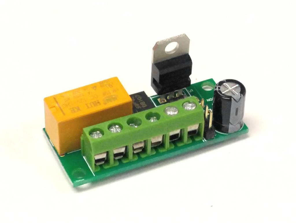
Of course, if you're building a circuit board anyway, a diode (or bridge), a TO-220 regulator and a decent filter cap will give you ultimate power flexibility, either AC or DC.  The selection of half-wave or full-wave power rectification will be based on the need (or lack of need) of a common ground with the input power source.

BTW MJCAT, there's no need to quote a fist full of graphics when they're right above, just makes the thread much bulkier.

Attachments

Images (1)
  • mceclip0
Last edited by gunrunnerjohn
stan2004 posted:

Is there any movement by component manufacturers to provide or translate their 3-D CAD data to make all this easier? 

I see more and more "360 view" in DigiKey and elsewhere for connectors and electro-mechanical parts so some effort is being made.

Stan: I've noticed the 3D views on Digikey as well. I tried to find a way to pick them up from their site but was unsuccessful. They sometimes include a CAD link in the description but that takes you to their KiCad library and application software; not the Step files used in DipTrace. Too many variations for 3D images I suppose.

GRJ: I have no idea how you manage to come up with this stuff. I followed your link to the GitHub repository and found numerous step files (.step or .stp). They contain a lot of ugly ASCII text that is not made for human consumption - as it says, Macros that programs turn into the 3D renditions.

I'm not about to get into kiCad. But the GitHub files are on the net and accessible. 

Congratulations on your excellent detective work. If I ever figure out how to use the component editor in DipTrace, I'll maybe attach some step files for the 3D images. Thanks once again.

Add Reply

Post
×
×
×
×
Link copied to your clipboard.
×
×